It is defined as the ability of a device to conform to its electrical and visual/mechanical specifications over a specified period of time under specified conditions at a specified confidence level
At the same time, It may represent a reputation of a company~
Hence,for the device a company develop and produce...For sure few reliability test will be done on it for the purpose of measuring the quality of bonds~~
What types of reliability test will be done a small chips??
- Visual Inspection
- Bond pull
- Bond Shear Test
- Bond Etching
- Electrical Testing
- Bake Test
- Thermal Cycle/Thermal Shock Testing
- Autoclave Testing
- Surface Anaylisis
- Temperature, Huminity, Bias (HTB)
**Some of this tests are usable as production monitoring techniques, where as some tests can only be used in the laboratory for evaluation and development of wire bond technology.
-This is a destructive test ( non-reversible process to test the strength of the specimen)
- The purpose of doing this test is to measure the metallurgical adhesion of the ball bond to the die pad
-The equipment used to perform this test are DAGE 4000 with BS500 catridge
BS 500 Cartridge
The procedures for ball shear test:
1.The shear tool has to be placed just beside the ball bond slightly above the surface of the first bond pad
2.The shearing arm then moves the tool horizontally against the ball which eventually pushes the ball off its bond pad.
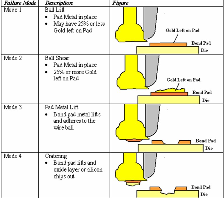
3.Readings, types of failure modes and pictures of failures are recorded.
Table for Ball Shear Test Failure ModesOptical Images After Ball Shear Test :
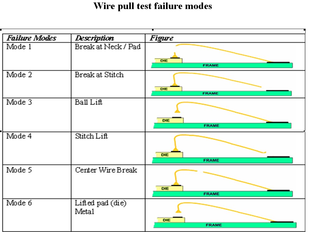
When I do the wire pull and wire peel test, there might be different failure mode.
Hence, while doing the testing I have to observe the failure mode at the same time and record it.
Some failure Mode may cause by the hook I using was bent, the pull & peel speed, the bonding parameter and etc...
The table for the failure mode is same for both wire pull and wire peel test!!
The step in doing the wire pull test
The wire pull hook was placed at the first kink (at the highest point along the loop of the wire), then the bonded wire was pulled away from the die with the hook.
The pulling force is usually applied perpendicular to the die surface. The breaking force is measured in gram.
Readings, types and pictures of failure mode are recorded
The steps in doing wire peel test
1.The hook is placed as close to the standardized position at the edge of the second bond pad as possible so that the failure will be at the second bond.
2.Normally wire bond at the corner of the chips will be chosen. This is due to the corner wire bonded is longest, hence weakest strength.
3.Readings, types of failure modes and pictures of failures was recorded. The failure modes are same as wire pull failure modes.
The wire at 2nd bond before wire peel test (top) and after wire peel test (bottom)
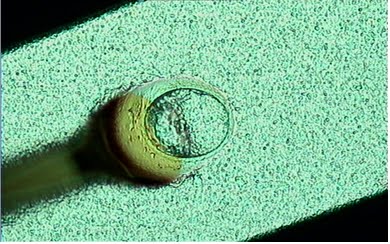
The photos below show the failure mode that may cause in the task, the photos in taken by using HISOMET :
From left to right : Lifted Ball. Break at Neck, Lifted Metal
Basically,this is the placement of the crescent of the second wire bond with respect to its designated substrate bond post.
The Photos show how the measurement have been done:
1. Place the green line on the left of the pad
2. Move the green line by rotate the X-axis.By doing so, i can get X1 value.
3. To find X2, same procedures have been done as step1&2 on the right side.
Crescent Width, W= PW-(x1+x2)
(c) Loop Height This test should be repeated for each grouping. For different grouping of wires, there are the specific limit for the wire. If the measurement is not within the limit, it is consider failed.
Cross-section view for different grouping of bonded wires: Layer1 - Ground
Normally, this two measurement will be found at the same time. The purpose for the test is to evaluate the shape and dimensions of the ball formed
BBD: 1. Measure the gold ball diameter(x&y axis) by setting the red cross line at the edge of the ball. Photo show the red line is putting at the left side and the bottom side of the bonded ball.
2. Then, it is move from left to right and bottom to up.
HISOMET is a machine that i used the most in my working life.
This is because HISOMET is used for :
(a) 1st bond placement measurement
(b) 2nd bond placement measurement
(c) Loop height
(d) Ball-bonded Height (BBD)
(e) Ball- bonded Diameter(BBH)
Let's talk about what is 1st bonded placement... ...
The two Cpk's will use actual measurements of the cone size, squashed ball size from the same ball bonds :
(a) Benchmark
The 2 photos show how I measure the cone size value for the left hand side, and same step will be done in right hand side.
The value that I get will use to get the Benchmarking Cpk.
(b) Internal
While this 2 photos show how I measure the squashed size value for the left hand side, and same step will be done in right hand side.
The value that I get will use to get the Internal Cpk.
In order to capture the range of the wire bond placement capability as fully as possible, there are a few considerations i have to take note in selecting which ball bonds to be measure : 1. Different groupings of wires Select ball bonds created from different groupings of wires
2. Different side of the dice Ball bonds from all four sides of the dice should be included
3. Location of dice on substrate strip Select dice that are far apart from each other on the substrate strip to measure the placement variation
4. Strip Select strips that were wire bonded at different times within an assembly lot. For example, select first strip. middle strip and last strip of a magazine
----------------------------------------To Be Continue--------------------------------------
As what i mentioned before, dage machine is used for wire pull,wire peel and bond shear test. The result i get from the wire pull and wire peel test are used for further analysis about the wire bond strength at the weakest point. While the bond test is for the evaluation and control of wire bond quality.
How should i construct the machine ??
This is the steps involve for ball shear test: (a) Substrate manually placed on fitting plate (b) Vacuum / window clamp holding by clicking "vacuum" in the program (C) Loading of shear system and program (d) Adjustment of tool in place of shearing - 2 controller(black color) :on the left side is used to control the fitting plate (left & right) on the right side is use to control the shear tool/hook ( up&down) (e) Press T, then the program will launch for automatic shears with specified programmable shear speed and sheer height. (f) Shear operation (g) Shear tool move up(0.15mm) then back to initial position (h) Data for each side of a unit are recorded
For the wire pull and wire peel test, the way i construct the machine is almost the same. BUT.... the main difference things is...it is using a hook and not a shear tool...
The difference between the wire pull and wire peel test is: For the wire pull test, the hook will placed at the first kink ( at the highest point along the loop of the wire), then the bonded wire will pull away from the die with the hook. For the wire peel test, the hook is place at the edge of the second bond pad ( * Corner part is the first choice to do this test because the wire at the corner is longest, hence the strength is the weakest)
I am supporting my supervisor which is using gold wire for wire bonding.To let me have an overall idea about the wire bonding process, my supervisor had bring me to walk around the production line mainly to produce Plastic Ball Grid Array (PBGA) and Tape Ball Grid Array (TBGA).
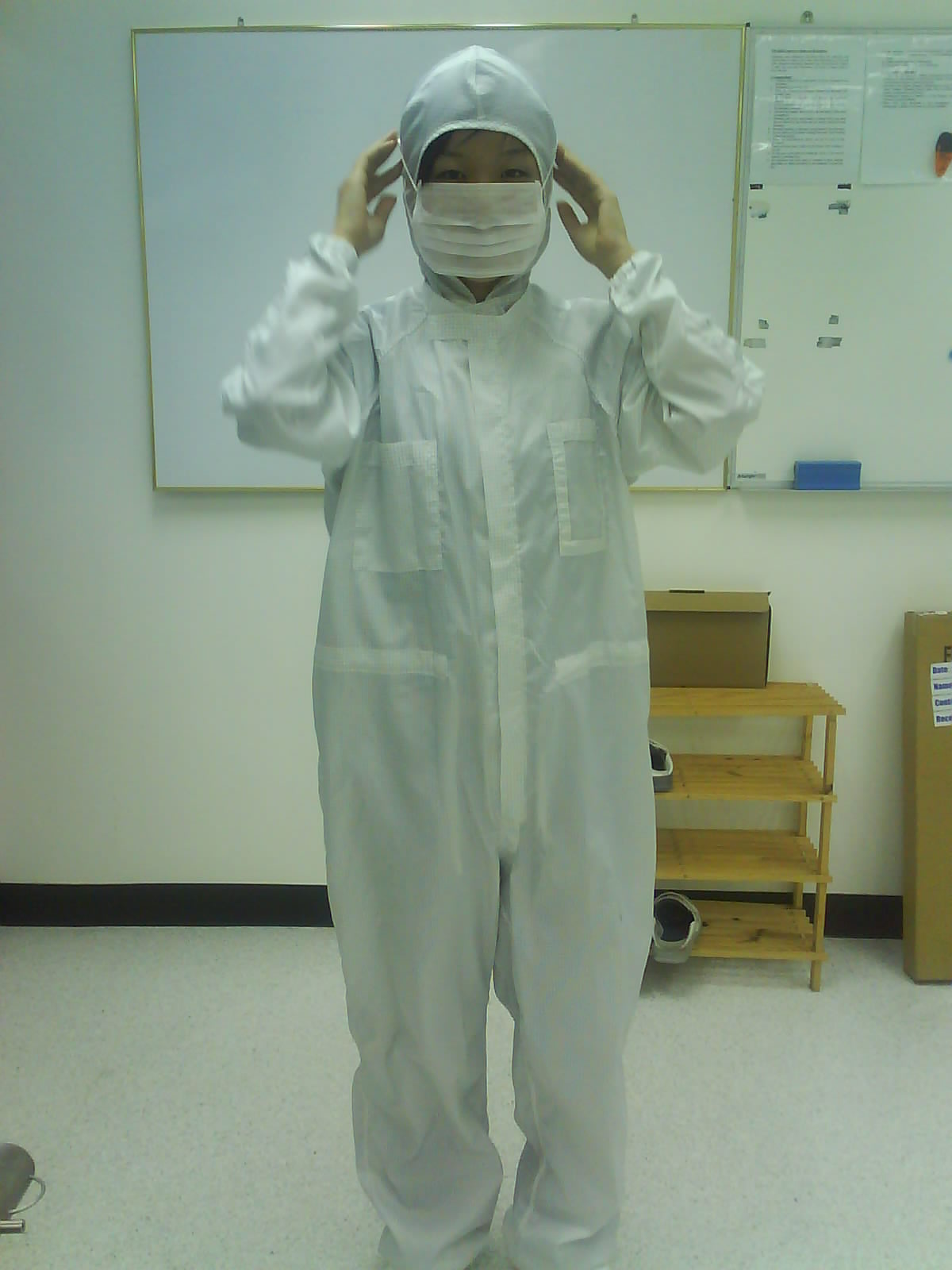
For PBGA, the balls are soldered on the back of the substrate on the specific location. While for TBGA, the solder ball is place around the die and not on the back of the substrate. **The entire work done in the production line need to wear Smock Suit. Features of Smock suit coverall: 1. Drop away electrostatic charge of human body 2. Friction voltage can be lower than 20V 3. It doesn't produce dust, doesn't absorb dust 4. Dressing comfortably, wash-fast, resistant to alkali and acid
Basically, wire bonding process is where a gold wire is use to connect the bond pad on the die to the substrate on the lead.
The process operate in the line include: (a)Substrate Preparation (to remove moisture on the substrate- pre cure for 150 Celcius) (b)Wafer Preparation - Wafer Dicing/ Wafer Sawing - Die Attach - Oven bake - Plasma Cleaning (c) Wire Bonding
"What is wire bonding?" This is the first question and the only question that most of us will ask our supervisor the most.
So, what is wire bonding?
Wire bonding is the process of providing electrical connection between the silicon chip and the external leads of the semiconductor devices using bonding wires.
Normally, wire usually used for the wire bonding is gold wire, aluminum wire and the copper wire.
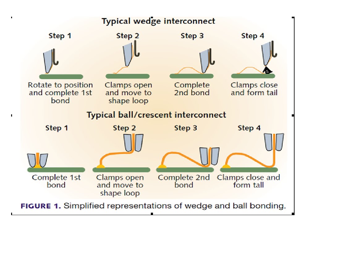
There are 2 types of bond methods:
(a) ball stitch
(b) wedge stitch
3 types of methods for imparting the requisite energy to attach wire to the bond site are :
(a) thermocompression (T/C)
(b) thermosonic (T/S)
(c) ultrasonic (U/S)
Department~ I have been assigned to work under Research & Development (R&D) department which mainly dealing with design of new package of semiconductor and test technology department.
Supervisor~ Every trainee in Freescale will be assigned to work under an engineer. My supervisor is Mr.Lee Boon Seong who are a Process Development Engineer. Hence, my job scope is basically conduct on the reliability and performance test.
Working Place~ The first day reporting to the company, i have tour around the company and Technology Solution Organization(TSO). This is the lab where most of my work done. There are HISOMET and DAGE MACHINE. Different equipments provide different function such as inspection,testing, cross sectioning and other tasks. Moreover, the wire pull and wire peel task also have to be done in this lab.
Figure above shows the hisomet machine which is used to do measurement on the placement of the wire bonding with the substrate.
Hisomet Result will be display on this screen The X, Y axis are used to find the 1st bond and second bond placement on the substrate. On the other hand, Z axis is used to measure the height of the wire bond. Measurement unit shown in either mm or inch.
Last but not least, figure below shows a dage machine that used to do wire pull, wire peel and ball shear test.
there is 24 hours in a day~ but at least 10 hours i will stay at the company~
It is more than 1/3 hours per day (**just applicable on weekdays,not weekends**)...haha~~
Let's have an overview about my second home~~
Freescale Semiconductor Malaysia
Freescale is actually a global leader in the design and manufacture of embedded semiconductors for the automotive, consumer, industrial, networking and wireless markets.
Launched as an independent company of Motorola, Freescale has the ability to serve customers more effectively through quicker decision-making, more efficient deployment of resources, increased flexibility and enhance responsiveness.
Freescale Semiconductor Malaysia, located in Petaling Jaya, is dedicated to assembly and testing of microprocessors, microcontrollers, digital signal processors, mixed signals and radio frequency (RF) integrated circuits (IC) for the Networking and Computing Systems, Transportation and Standard Product Systems and Wireless & Broadband Systems market segments.
So, this is the company where i am going to have intern for 12 weeks.......
I am undergoing my internship at Freescale Semiconductor Sdb.Bhd from 5April-25June 2010.
My working hour is from 8am-5.30pm..
I thought i can wake up at 7.30am..
BUT...
i CAN'T!!
i have been suggested to wake up at 6am and get ready to AVOID traffic jam~!
Oh my~~6am is still a time for me to stay with my lovely bed..It's too cruel to leave it alone so EARLY.
BUT..
there is another choice for me....What's that?? waiting... waiting the suggestion...with happy mood...
The next choice is u may wake up at 7am(wow,is GOOD~i LOVE it)....
but stuck in jam for an hour(i HATE this)...T.T
So, what will you choose?? That's y people always say no 100% perfection in life~! i am in dilemma~~ @.@


 THE END ~HIsOmET~!